[ Instrument Network Instrument R & D ] The High Magnetic Field Science Center of the Hefei Institute of Material Science, Chinese Academy of Sciences, and the Institute of Quantum Materials and Physics of Anhui University cooperated with a low-temperature strong magnetic field scanning tunneling microscope / spectroscopy (STM / STS) The chalcogenide compound 2H-NbSe2 and its trace Ta-doped single crystal samples were investigated. The researchers confirmed the existence of inelastic electron tunneling in the system through high-resolution tunnel spectrum measurement and theoretical analysis of the system. At the atomic scale, the electro-phonon coupling spectrum function of a system is identified. Related research was published in the Physical Review Letters on March 13.

Transition metal chalcogenide (TMD) is an important branch of two-dimensional materials. It has adjustable intrinsic band gap and valley degrees of freedom. It has great application prospects in the fields of electrical, optical, and spintronics devices. 2H-NbSe2 is a typical TMD material. As a representative of the coexistence system of charge density wave (CDW) and superconductor, it is also one of the materials widely studied by STM. For nearly 30 years, the cause of the inflection point at ± 35 mV in the tunnel spectrum of this system has always puzzled researchers in this field, and has also become an obstacle to understanding the mechanism of charge density waves.
The phonon is the most typical representative of the collective element excitation of solid materials. It describes the simple harmonic oscillator of the quantized collective atomic motion. The thermal and electrical properties of materials, and even superconductivity and charge density waves are closely related to phonons, especially electron-phonon interactions. When a strong electron-phonon interaction exists in the material, an inelastic electron tunneling process may occur between the STM tip and the sample, that is, as the tunnel bias increases, the electrons have sufficient energy and can pass through the excitation. The phonons in the material reduce the energy, open a new tunneling channel, resulting in an increased tunneling probability, which is manifested by a sudden increase in the slope of the IV curve of the tunnel junction. Accordingly, a step appears on the dI / dV curve. A sub-differential d2I / dV2 curve appears as a peak (valley at negative bias).
After the joint research team grew high-quality 2H-NbSe2 and a small amount of Ta-doped single crystal samples, they performed high-resolution tunnel spectrum measurement through a low-temperature strong magnetic field STM / STS, and found that the tunnel spectrum has complex fine structures within ± 35mV .
Theoretical research shows that the quadratic differential curve is approximately proportional to the electrophonon coupling spectral function α2F (ω). Therefore, this STM-based inelastic electron tunneling spectrum (IETS) method can be used for electrophonon coupling at the atomic scale. Research. However, due to the experimental requirements for high resolution and the characteristics of the material itself, the current successful cases are limited to very limited solid materials, such as graphite or graphene, metallic copper, etc.
Subsequently, the researchers proposed a concise theoretical model by calculating the electrophonon coupling spectral function. Model calculations and analysis confirm that these fine features (including the confusing ± 35mV inflection point) come from the inelastic electron tunneling process, eliminating the misinterpretation of the CDW energy gap at ± 35mV for many years.

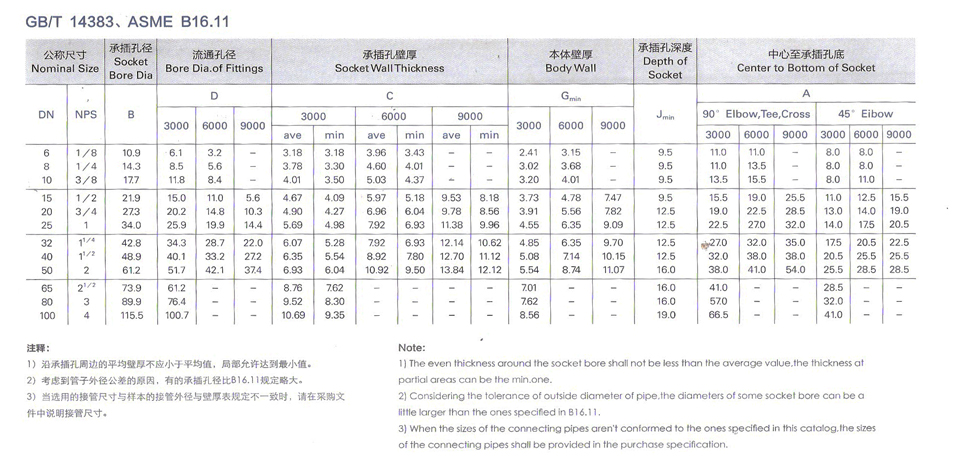
Socket Weld 45Ded Elbow,Socket Weld Elbow High Pressure,Socket Weld 90D Elbow,Forged Socket Weld 45D Elbow
Wenzhou Kezheng Valve Pipe Fitting Co., Ltd. , https://www.kezhengfitting.com